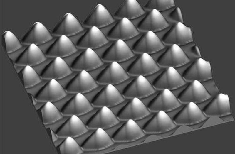
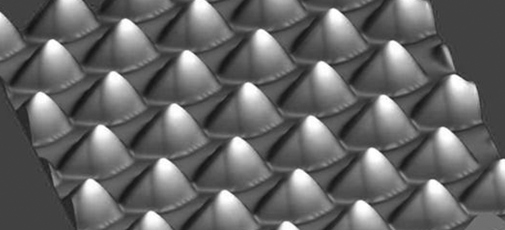
Patterned Sapphire Substrates (PSS) is a micro-patterned sapphire substrate used for GaN-based light-emitting diodes(LEDs). PSS with small structures greatly improves the light extraction efficiency of finished devices. PSS also solves critical problems such as crystal dislocations and refractive index mismatch.
There are two different manufacturing processes to fabricate PSS in the industry, dry plasma etching and wet chemical etching. Today, the majority of PSS products are produced by dry plasma etching due to its inherently effective control of precision and uniformity.


| Item | 4-inch C-plane(0001) 650μm Pattern Sapphire Substrate |
| Crystal Materials | 99,999%, High Purity, Monocrystalline Al2O3 |
| Grade | Prime, Epi-Ready |
| Surface Orientation | C-plane(0001) |
| Diameter | 100.0 mm +/- 0.1 mm |
| Thickness | 650 μm +/- 25 μm |
| Primary Flat Orientation | A-plane(11-20) +/- 0.2° |
| Primary Flat Length | 30.0 mm +/- 1.0 mm |
| Pattern Specification | Diameter: 2.7 +/- 0.1 μm; Spacing: 0.3 +/- 0.1 μm; Depth: 1.7 +/- 0.15 μm |
| Front Surface | Epitaxial ready |
| Back Surface | Fine ground, Ra = 0.8 μm to 1.2 μm |
| Laser Marking | Front side or Back side |
| TTV | < 20 μm |
| BOW | < 20 μm |
| WARP | < 20 μm |
| Cleaning / Packaging | Class 100 cleanroom cleaning and vacuum packaging, |
| 25 pieces in one cassette packaging or single piece packaging. |
CRYSCORE offers high-quality patterned sapphire substrates, and we have customized solutions for you, get in touch with us now!
 An Introduction to Silicon on Sapphire Technology
 Coating and Metal Coating of Sapphire Windows
 Introduction to the Manufacturing Process of Sapphire Ingot