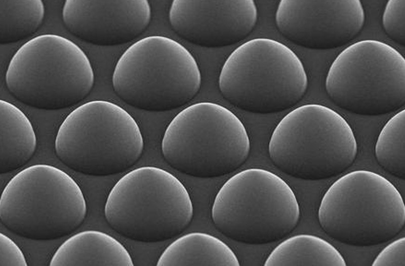
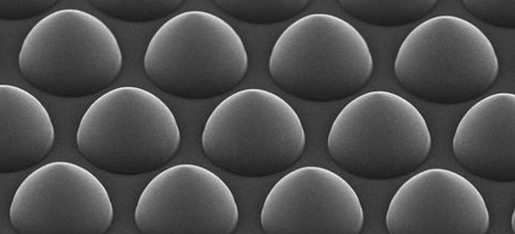
PSS is to design and manufacture specific nano-scale microstructure pattern on the sapphire substrate, in the way of growth and etching, to control the form of LED light output (the concave and convex pattern on the sapphire substrate will produce a light scattering or refraction effect to increase the extraction rate of light).
Meanwhile, GaN thin film growing on the patterned sapphire substrate will produce the effect of lateral epitaxial, reduce the gap defects between GaN and sapphire substrate, improve the quality of epitaxy, and promote the LED inside quantum efficiency and increase light-extraction efficiency.


| Item | 2-inch C-plane(0001) 430μm Pattern Sapphire Substrate |
| Crystal Materials | 99,999%, High Purity, Monocrystalline Al2O3 |
| Grade | Prime, Epi-Ready |
| Surface Orientation | C-plane(0001) |
| Diameter | 50.8 mm +/- 0.1 mm |
| Thickness | 430 μm +/- 25 μm |
| Primary Flat Orientation | A-plane(11-20) +/- 0.2° |
| Primary Flat Length | 16.0 mm +/- 1.0 mm |
| Pattern Specification | Diameter: 2.4 +/- 0.2 µm; Spacing: 0.6 +/- 0.2 µm; Depth: 1.5 +/- 0.15 µm |
| Diameter: 2.7 +/- 0.1 μm; Spacing: 0.3 +/- 0.1 μm; Depth: 1.7 +/- 0.15 μm | |
| Front Surface | Epitaxial ready |
| Back Surface | Fine ground, Ra = 0.8 μm to 1.2 μm |
| Laser Marking | Front side or Back side |
| TTV | < 10 μm |
| BOW | < 10 μm |
| WARP | < 10 μm |
| Cleaning / Packaging | Class 100 cleanroom cleaning and vacuum packaging, |
| 25 pieces in one cassette packaging or single piece packaging. |
If you are looking for reliable sapphire substrate manufacturers, choose us to be your partner and we'll make it worth it.
 An Introduction to Silicon on Sapphire Technology
 Coating and Metal Coating of Sapphire Windows
 Introduction to the Manufacturing Process of Sapphire Ingot